Technical PV Outlook: What your module supplier should be on track for?
Reducing manufacturing cost to its minimum
For years now the PV manufacturers have managed to drastically cut down the cost of photovoltaics in many ways, by vertical integration & supply optimisation but more importantly by developing process and technology innovations. Top manufacturers have understood that. Here are the trends of their current process and product development.
Diamond sawing cutting the mono wafer costs
Among the innovations recently industrialized, one indubitably has a big impact on cost breakdown: Diamond Wire Sawing. Higher sawing speed, lower kerf* loss (60 wafers/kg vs. 49 wafers/kg with slurry based sawing) are the reasons why this process has rapidly become mainstream for Mono and still ongoing for Multi which is facing some uniformity imperfections, high reflective areas on the wafer surface and texturing challenges.
Black silicon process for Multi wafer as described later will solve those issues.
On top of that, as the process is less energy consuming the environmental impact is better which can make the difference on certain markets (French CRE tenders).
Multi with Black silicon to catch up with mono
To catch up with Mono’s efficiencies, R&D has spent efforts on developing Black Silicon for Multi cells which is becoming more and more popular nowadays. This technic consists in etching nanoscale craters on the surface of the wafer which makes it more uniform and very low-reflective increasing the cell efficiency up to 0,8%. Two different process have been developed to do so, Reactive Ion Etching (RIE) commonly called “dry etching” and Metal Catalysed Chemical Etching (MCCE) called “wet etching”.
Whereas the first one was developed and industrialized earlier, the second is now ready and allow higher cost reduction with reasonable efficiency gain.
Progressively solving LID for mono & multi cells
Another remarkable optimisation which has been developed by the UNSW is Advanced Hydrogenation**. This consists in boron-oxygen defects passivation (responsible of LID losses) in Czochralski silicon by applicating laser hydrogenation to the finished solar cell. Last results have shown a 1,1% absolute efficiency gain on PERC p-type Mono cells and no LID. Solution are now being implemented all over the world on mono PERC lines. This process also works for n-type technology.
Further work has been done with multicrystalline technology which has a larger range of defect making hydrogen passivation more difficult. UNSW research have been successful and solution will be release this year for future LID free p-type PERC multicrystalline modules commercialization.
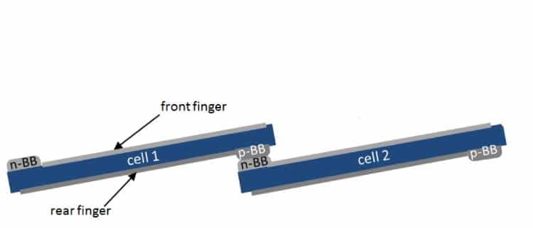
Copper Plating, the screen printing alternative
Manufacturers have progressively optimized screen printing to consume less silver paste and reduce shadings. Nevertheless, a limit has been reached as a certain wide must be respected to obtain sufficient electrical conductance. Copper plating answers that issue allowing narrower lines, Ag savings and less series resistance to obtain an absolute efficiency gain of 0,5%. This process is highly suitable with new cells architecture such as PERC, IBC or MWT. Modules with copper plated cells have already passed the IEC61215 certifications and copper plating lines are available. The technology will gain some market shares (~4% for 2019) but screen printing metallization remains mainstream.
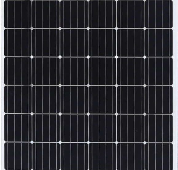
New module designs for higher output and specific applications
At the module level, alternative designs have been found to decrease the CTM losses and reduce manufacturing cost. Half-cells and shingled cells modules have appeared on exhibition catching the attention by their different aspect. Such assembling of cells permits series resistance reduction and higher power density. An extra output power of +5W is reached on a 60 cells module.
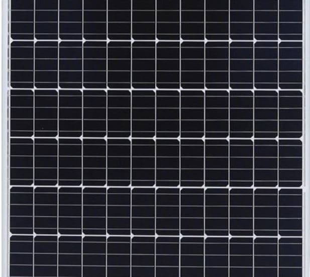
Multi busbar technology is also ready for commercialisation. Developed by SCHMID, the technology allows the soldering of cells with 12 wires. Main advantages are shadings and series resistance reduction leading to a +10W power output for a 60 cells module. Moreover, silver paste consumption can be decrease up to 50% in cell production.
Driven by the aviation industry “no glass” PV crystalline modules are also being developed. These products are answering the needs of industrial buildings that can’t allow more weight on their roof without costly reinforcements and facilitate specific curved integration. Flexible and light (<2,5 kg per square meter***) mountings method and application are very diversified (standard mounting on substructure, glued, screwed, using magnets…)
Looking ahead
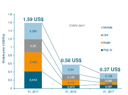
Led by this dynamic of continuous process and product improvement, manufacturing cost of the watt peak will rapidly reach 0,30$ if we listen to the top actors of the PV manufacturing industry. This is just the beginning and the challenge of producing the most affordable energy for everyone is now realistic if you make sure your PV supplier is on track for it.
CRE Commission de Régulation de l’Energie
LID=Light Induced Degradation
PERC=Passivated Emitter Rear Contact
IBC=Interdigitated Back Contact
MWT=Metal Wrap Through
CTM=Cell To Module
*cutting waste
**http://www2.pv.unsw.edu.au/videos/Stuart-Wenham-8December2016/slides/SPREE-Alumni-Event.pdf